
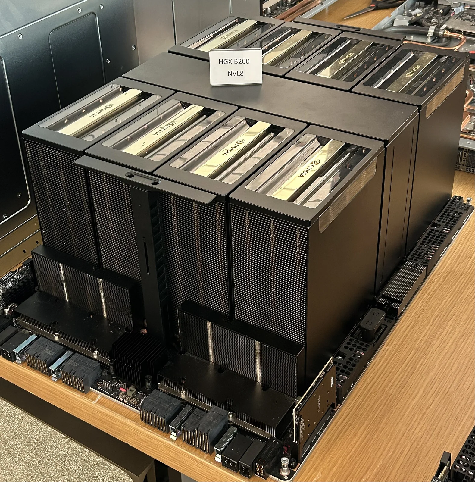
In NVIDIA’s DGX stack the firmest lock-in is not in the GPU but in the interconnect between GPUs: NVLink and NVSwitch define a proprietary coherent memory domain, while the layers around that domain — the software (NCCL) and the rack mechanicals contributed to the Open Compute Project — are published and reusable. The difference between the two planes surfaces as soon as you size a training cluster or weigh an exit path.
Context: how the NVLink domain grew
The DGX line began in 2016 as a turnkey training server: eight Tesla P100 (Pascal) GPUs wired in a hybrid cube-mesh topology over first-generation NVLink. That topology has a limit: not every GPU reaches every other GPU at full bandwidth in a single hop, some pairs route through intermediate nodes.
The DGX-2 (March 2018) removes that limit with NVSwitch, a crossbar chip linking 16 V100 GPUs into a fully non-blocking NVLink fabric: every GPU reaches every other in a single hop, with 300 GB/s of aggregate bidirectional bandwidth per GPU across 6 NVLink 2.0 links at 25 GB/s each (NVIDIA Developer Blog, NVSwitch Accelerates NVIDIA DGX-2). The system shows one job 512 GB of HBM2 memory as a single space. Here the NVLink domain stops being a cabling detail and becomes the unit of design.
Later generations widen that domain. DGX A100 (2020) carries eight A100 GPUs with six NVSwitches and adds MIG to partition each GPU into seven isolated instances. DGX H100 (2022) moves up to eight H100 GPUs with third-generation NVSwitch and ConnectX-7 NDR at 400 Gb/s. In all these configurations the NVLink domain stays closed to eight GPUs per node: beyond that threshold communication routes over InfiniBand, where latency and bandwidth shift by an order of magnitude.
The scale jump arrives with GB200 NVL72, shown at GTC on 18 March 2024: a liquid-cooled rack with 36 Grace CPUs and 72 B200 GPUs linked by an NVLink Switch System that takes the coherent domain to 72 GPUs, with 1.8 TB/s of NVLink bandwidth per GPU and 130 TB/s aggregate in the fabric (NVIDIA product page, GB200 NVL72). To software, the rack behaves as one very large GPU.
Architecture: where the line falls
Separating three planes helps see what is really tied down.
The interconnect silicon plane — the NVLink protocol and the NVSwitch chips — is proprietary and undocumented at protocol level. There is no second source: no third party builds an NVLink switch, and no non-NVIDIA accelerator joins an NVLink domain. This is where the vendor tie concentrates, because it is the interconnect topology, not the individual GPU, that decides which models train without manual memory sharding.
The collective software plane, by contrast, is open. NCCL (NVIDIA Collective Communications Library) implements all-reduce, all-gather, reduce-scatter, broadcast and the point-to-point patterns every distributed training framework rests on; it ships under a three-clause BSD licence, with source public on GitHub (NVIDIA/nccl). At bootstrap NCCL builds rings and trees matched to the topology it detects — NVLink inside the node, GPUDirect RDMA over InfiniBand between nodes, TCP/IP as a fallback — and that construction logic is readable. The layer PyTorch or JAX call to synchronise gradients can therefore be inspected, even when it runs over a closed fabric.
The rack mechanical and electrical plane is partly open. At the 2024 OCP Global Summit NVIDIA contributed to the Open Compute Project the designs of the GB200 NVL72 rack and of the liquid-cooled compute and switch trays: rack architecture, tray mechanicals, thermal and liquid-cooling specifications, the volumetrics of the NVLink cable cartridges (NVIDIA Developer Blog, NVIDIA Contributes NVIDIA GB200 NVL72 Designs to Open Compute Project). These designs derive from the MGX architecture, and with them third-party integrators — the OCP catalogue lists racks from Pegatron and others — build compatible chassis without redrawing the mechanicals. What stays outside the contribution is precisely the protocol that runs inside those cable cartridges.
The critical point: the coherent domain as the unit of lock-in
In a DGX cluster the vendor tie is not measured by counting GPUs. It is measured against the size of the NVLink domain a single model demands. A model that fits in the aggregate memory of eight GPUs runs on any OEM-baseboard HGX H100 server (Supermicro, Dell, Lenovo) — same silicon, same NCCL, eight-GPU NVLink domain — and largely on competing accelerators too, because the collective layer is portable. A model that asks for a coherent 72-GPU domain, by contrast, exists as a runnable workload only on an NVL72: there is no non-NVIDIA equivalent of an NVLink fabric at that scale, and reconstructing the same memory coherence over InfiniBand changes the bandwidth and latency profile to the point where the training code registers it.
It follows that the architectural decision with the highest exit cost concerns model size before it concerns the choice of GPU: designing a model whose memory working set exceeds the NVLink domain available on multi-vendor hardware ties you to a single fabric. That threshold — today eight GPUs on second-source silicon, 72 on the single-source NVL72 fabric — is the real boundary.
Implications
For anyone sizing training infrastructure, the open layer is worth using where it cuts the tie and worth ignoring where it does not. NCCL under BSD means the synchronisation code is verifiable and that collective tuning does not depend on an opaque binary; the OCP contribution means the rack mechanicals have more than one supplier. Neither, though, opens the NVLink protocol: the portability of a workload stays set by the size of the coherent domain the model demands.
From this a sober design rule: keep model working sets inside an NVLink domain reproducible on second-source silicon while requirements allow, and treat the jump to an NVL72 domain as an explicit vendor-tie decision, not a plain capacity step.
Limits
The distinction between the three planes describes the state on 18 March 2025 and does not anticipate roadmap. The Blackwell Ultra platforms announced today at GTC — GB300 NVL72, and the DGX Station and DGX Spark workstations — keep the same model: closed interconnect silicon, open NCCL, rack mechanicals partly contributed to OCP. The bandwidth and capacity figures cited come from NVIDIA material and third-party technical blogs, not from independent measurement under load; read them as vendor claims. The open software layer considered here is the collective alone: the CUDA driver, NVSwitch firmware and GPU microcode remain proprietary binaries, and fall outside what can be inspected or replaced.
- https://developer.nvidia.com/blog/nvswitch-accelerates-nvidia-dgx2/
- https://www.nvidia.com/en-us/data-center/gb200-nvl72/
- https://developer.nvidia.com/blog/nvidia-contributes-nvidia-gb200-nvl72-designs-to-open-compute-project/
- https://github.com/NVIDIA/nccl
- https://developer.nvidia.com/nccl
- https://nvidianews.nvidia.com/news/nvidia-contributes-blackwell-platform-design-to-open-hardware-ecosystem-accelerating-ai-infrastructure-innovation
- https://www.noze.it/en/insights/nvidia-dgx-platform/
Cover image: NVIDIA HGX B200 eight-GPU baseboard: a large square board carrying eight mounted Blackwell GPU modules with dense heat sinks and… — photo by Pokiiri, CC BY-SA 4.0 — https://commons.wikimedia.org/wiki/File:Nvidia_DGX-B200-HGX.jpg