
The Jetson Nano Developer Kit announced today at GTC 2019 exposes the same nvcc, the same cuDNN and TensorRT that run on a datacentre Tesla, inside a 5-10 W module that costs 99 dollars (NVIDIA Developer Blog). For anyone designing systems what counts is not the price. It is the continuity of the compilation stack between the hardware a network is trained on and the hardware that network runs on at the edge.
Context
The Jetson family dates from 2014: first the TK1, then TX1 and TX2, up to the Xavier shown in 2018. These were modules from 200 to over 600 dollars, aimed at robotics and industrial products. The entry-level segment of embedded computing was instead the ground of general-purpose boards — Raspberry Pi 3, the various ARM boards — where a convolutional network runs inference on the CPU, with latencies that make real-time video processing impractical.
The Jetson Nano sits below the TX1 in the hierarchy and reuses much of its SoC. The continuity with the rest of the line is stated outright: the same JetPack (version 4.2 at launch, built on Ubuntu 18.04) flashes the image onto Nano, TX2 and Xavier alike (NVIDIA Developer Blog).
Architecture
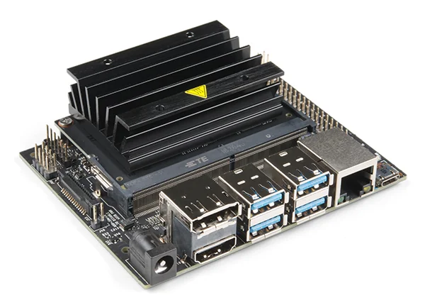
The specifications stated at launch:
- GPU: 128 Maxwell CUDA cores at 921 MHz, 472 GFLOPS in FP16
- CPU: quad-core ARM Cortex-A57 at 1.43 GHz
- RAM: 4 GB LPDDR4 at 1600 MHz, 25.6 GB/s of bandwidth
- Four USB 3.0 ports, Gigabit Ethernet, HDMI and DisplayPort
- 40-pin GPIO header with a Raspberry Pi-compatible pinout (3× I2C, 2× SPI, UART, I2S)
- Two 15-pin MIPI CSI-2 camera connectors
- Hardware encode up to 4Kp30, decode up to 4Kp60
- 5 V supply, 5 W and 10 W power modes
The 128 Maxwell cores are the same microarchitecture as the 2014-2015 GeForce 900 parts. Here is the point: a CUDA kernel compiled for sm_53 (the Tegra X1’s compute capability) uses the same execution model — warps, shared memory, registers per block — as any discrete Maxwell. The difference is quantitative — 128 cores against the thousands of a desktop GPU — not qualitative.
The software stack at launch comprises CUDA Toolkit 10.0, cuDNN 7.3 and TensorRT 5, plus OpenCV and ROS in the JetPack image (NVIDIA Developer Blog). The training frameworks usable for inference run from TensorFlow and PyTorch to Caffe, Keras and MXNet.
The critical point
The practical value lies in a training-to-deployment chain with no rewrite of the compute kernel. A model trained on a desktop GPU produces weights that TensorRT optimises for the Nano target: it fuses the layers, picks the kernels for sm_53, quantises from FP32 to FP16. The Tegra X1’s Maxwell GPU runs FP16 at twice the rate, and on this hardware that becomes the reference precision for inference.
There is no ready-made binary compatibility: the model still goes through TensorRT, or is loaded from the framework and recompiled for the target. The compatibility sits at stack level — the same APIs, the same compiler, the same memory model used on the server. Anyone who already has a CUDA pipeline need not adopt a separate runtime to take inference to the edge, as would happen moving to an accelerator with a proprietary toolchain.
From here come the Nano’s two real constraints. The first is memory: the 4 GB of LPDDR4 are shared between CPU and GPU. A network like ResNet-50 in FP16 sits well within the budget, but larger detection models, or several networks in parallel, force you to profile occupancy and often to lower the input resolution. The second is bandwidth: 25.6 GB/s sits an order of magnitude below a desktop GPU’s bandwidth, so memory-bound layers — pooling, normalisations, element-wise activations — do not scale as the compute-bound ones do.
Implications
For edge computer-vision workloads the Nano shifts the balance between local processing and sending to the cloud. An IP camera that today ships its stream to a server for detection can run the same network locally and send only the events. Network bandwidth drops, latency drops, raw-data exposure drops — and the last of these counts when the stream contains faces or number plates and you would rather not transmit them.
The 99-dollar price also moves where it pays to prototype. A dissertation, an industrial proof-of-concept, a ROS robotics experiment run on real hardware rather than on an emulator or on rented GPU time. Since the stack is the same, the code that runs on the prototype Nano will run on a Xavier in production, bar re-profiling the performance.
It pays to separate the technical marketing from operational reality. The stated 472 GFLOPS is a theoretical peak in FP16. Real throughput on a real network depends on kernel efficiency, memory occupancy and the power mode: at 5 W the GPU clock drops below the nominal 921 MHz, and the published frames-per-second figures take for granted the 10 W mode with TensorRT optimisation applied.
Limits
The Nano is not a training platform: 128 cores and 4 GB are enough to fine-tune small networks, not to train realistic-sized models from scratch. Maxwell, moreover, is a 2014 microarchitecture: it lacks the Tensor Core that arrived with Volta in 2017, so the dedicated INT8 acceleration and mixed-precision operations of more recent accelerators are absent. The camera requires MIPI CSI-2-compatible sensors, otherwise you go through USB, and Wi-Fi is not integrated — an M.2 module has to be added.
What stays verifiable as of today is that the same CUDA toolchain that compiles for a datacentre compiles for a 5-watt module, and this is the first point on the Jetson line where that toolchain costs less than an entry-level graphics card.
https://developer.nvidia.com/blog/jetson-nano-ai-computing/ https://developer.nvidia.com/embedded/jetson-nano https://www.cnx-software.com/2019/03/19/nvidia-jetson-nano-developer-kit/ https://www.noze.it/en/insights/nvidia-jetson-nano/
Cover image: Top-down view of the NVIDIA Jetson Nano developer board: a PCB with a black finned heatsink in the center, a 40-pin GPIO header, and… — photo by SparkFun Electronics, CC BY 2.0 — https://commons.wikimedia.org/wiki/File:NVIDIA_Jetson_Nano_Developer_Kit_(47616885631)_(cropped).jpg